A cost-efficient approach to realize analytical systems
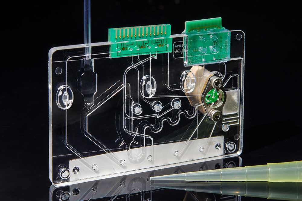
Polymer materials are an indispensable part of, in particular, microfluidic and optical analysis applications. Compared to glass and silicon they are considerably cheaper and can be economically structured at large scale as well as at small scale. Depending on the application there is a selection of different materials that is worth considering. These can additionally be matched even more precisely to the enquiry by an appropriate surface treatment. We have long-time practical experience with the realization of microstructured polymer parts, for instance microfluidic chips, polymer waveguides, micro gear systems or micro lenses. We guide you through the entire process from the idea generation via molding techniques, assembly and packaging technologies and surface treatment up to small series
Your advantage
- Fabrication or sampling of prototypes up to small/pilot series,
- feasibility studies of complex fabrication processes up to their optimization,
- upgrading of components by post processing or the implementation and application of functional elements,
- multilayer covering of tiniest structures.
Our success factors
- More than 20 years of practical experience,
- highly qualified interdisciplinary team,
- close cooperation with the customer.
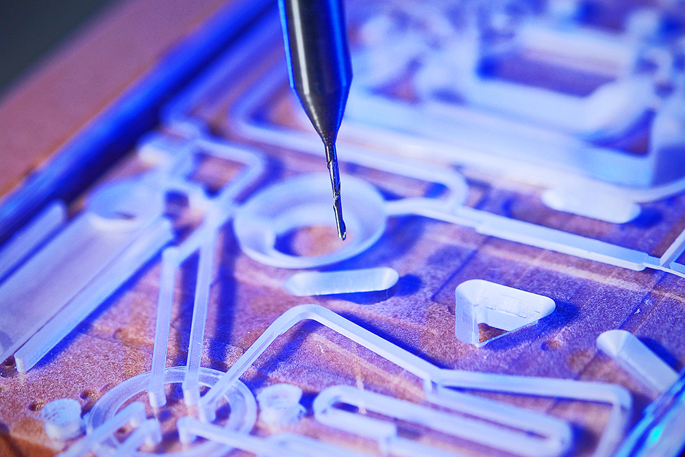
We are experts in high level tool making and the realization of mold inserts for hot embossing and injection molding, whether via lithographic or fine mechanical technologies. The process portfolio we have at our disposal comprises cutting precision engineering, laser material processing, 3D and screen printing processes, plasma treatment, spotting, hot embossing or injection molding. We have extensive experience in assembly and packaging technologies for the realization of (hybrid) complete systems. This includes the covering of multilayer polymer channels, die integration of lithographically structured silicon and glass components, applying metal layers/electrodes or the incorporation of membranes and filters. Furthermore, we have experience with surface modification procedures, such as the polishing of surface roughness or the local functionalization with biomolecules.
Our equipment:
- Precision mechanical workshop,
- high-performance lasers for material processing (cutting, ablation, welding),
- hot embossing system HEX01 by Jenoptik,
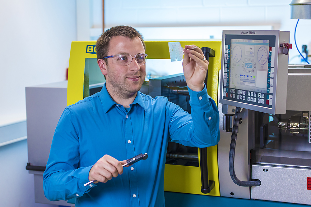
- injection molding machine Boy35E,
- 3D printer German Rep Rap X400,
- screen-printing installation,
- spotter.
Typical application examples
- Structuring, mounting and covering of microfluidic polymer systems,
- molding of polymer waveguides and other microoptical structures,
- incorporation of membranes/electrodes/ silicon parts in polymer components for various tasks, such as microfluidic lab on a chip systems,
- construction of complex microfluidic chip systems taking into account long-term stability of liquid or freeze dried reagents and further bio physical impacts of materials,
- transfer from conventionally produced prototype components into components capable for injection molding allowing initial samples.
 Fraunhofer Institute for Microengineering and Microsystems IMM

