Energy from the solar plasma

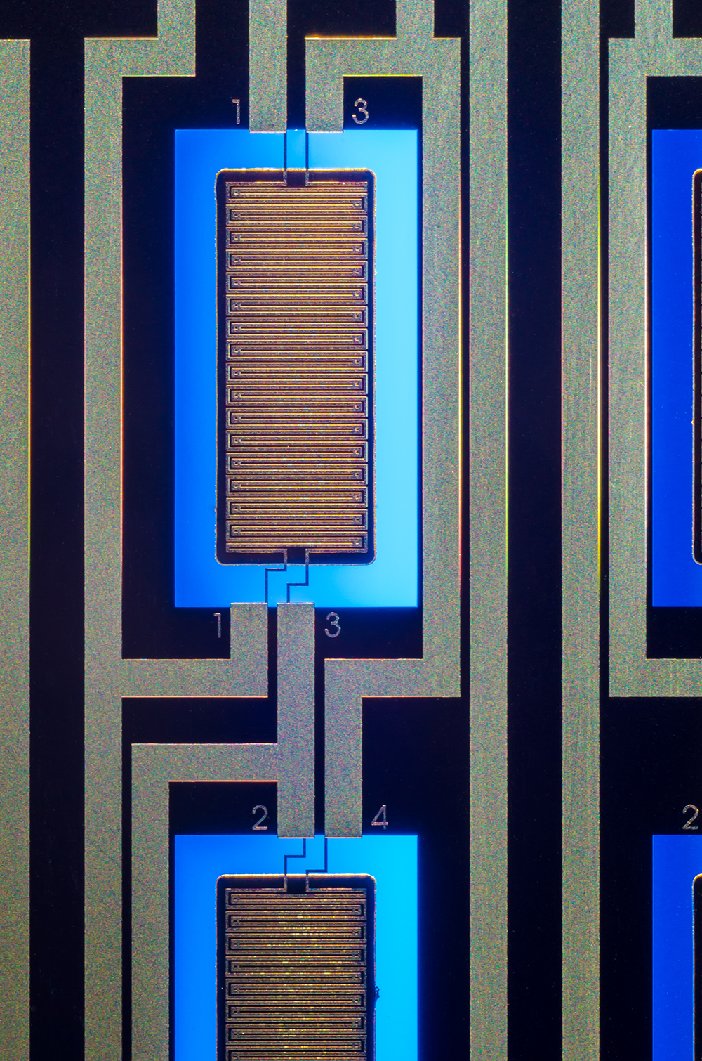
By means of nuclear fusion, i.e. the fusion of two light atomic nuclei, a considerable amount of energy can be gained from only very small quantities of „combustion material” such as deuterium and tritium. However, the nuclear fusion reaction demands considerable technical effort to generate an extremely hot, magnetically confined fusion plasma as well as precise monitoring and control of the respective processes. This includes for instance the determination of the plasma radiated power at different points of the containment. For this purpose, special radiation sensors known as bolometers are used. In many of the fusion research plants operated around the world these radiation sensors nowadays come from us.
Functionality
Bolometers usually rely on a gold or platinum absorber with a thickness of up to some 10 microns depending on the maximum radiation energy to be detected. Precise measurement of the temperature increase resulting from the radiation absorption is provided by a temperature-dependent, precision platinum resistor located on the back side of the absorber.
Challenges for use at ITER
At the world's largest fusion experiment "ITER" which is currently under construction, very harsh environmental conditions will prevail. In particular, changing thermal loads up to 450 °C together with high radiation levels represent substantial challenges. Therefore, existing bolometers can be used only to a limited extent. In cooperation with the Max-Planck Institute for Plasma Physics in Garching, we have made significant steps towards a new generation of more reliable bolometer sensors able to match the extreme operation conditions at ITER. By using alternative materials and a new concept for mechanical fixation of the sensor structure by flexure hinges, a temperature stability of up to 450 °C could be verified in preliminary tests.
Our research & development services
Both, the skills and expertise of our process engineers and a well-equipped cleanroom facility for silicon micromachining, assembly and metrology provide the basis to transform innovative ideas into new product applications. Our customers come from industrial instrumentation and analytics, medical device manufacturing, biodiagnostics, aerospace and cutting-edge research.
Further current application developments for silicon-based components are:
- Microfluidic density measurement for liquids,
- flow rate sensors,
- 3D tactile force sensors,
- silicon micromachined precision components,
- micro electrode structures.
 Fraunhofer Institute for Microengineering and Microsystems IMM