 Fraunhofer Institute for Microengineering and Microsystems IMM
Precision and speed give a competitive edge in modern manufacturing
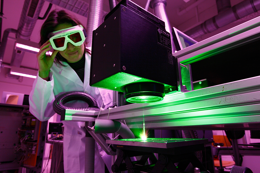
In modern manufacturing such as welding of chassis parts in automotive industry, surface treatment in tooling industry or cutting in solar cell industry, lasers have become essential. The contactless processing without transmission of force as well as the high accuracy and speed are only some of the features that make the use of a laser attractive to microtechnological applications. With suitable methods even structures in the nanometer range can be achieved. These methods include two-photon-absorption or interference lithography.
Your advantage
Our long-time experience in laser micromachining is the basis from which we elaborate individual solutions in the course of our cooperation with project partners. We offer to conduct technological feasibility studies, the realization of functional models as well as the fabrication of pilot series. If desired, we arrange a technology transfer or build up systems which are tailor-made to meet the requirements of our customers.
Our equipment
We use a range of lasers for the realization of most tiny structures as well as in microtechnological assembly and packaging technology.
- excimer laser, 193 nm, 10 W, 300 Hz, tp=5 ns,
- Nd:YAG disk laser, 1064 nm, 1 kW, cw
- Nd:YAG laser, 1064 nm, 60 W, cw+50 kHz, tp=100 ns
- Nd:YAG laser, 1064 nm, 120 W, 40 Hz, tp=0,3-20 ms
- Yb:YAG laser, 1030 nm, 25 W, 600 kHz, tp=5 ps
- diode laser bar, 976 nm, 30 W, cw
- Nd:YAG laser, 1064 nm, 40 W, 40 Hz, tp=0,3-20 ms
- Nd:YAG laser, 532 nm, 18 W, 30 kHz, tp=15 ns
- CO2 laser, 10,6 µm, 30 W, 1 kHz, tp=1 ms
- Ti:Sapphire laser, 800 nm, 200 mW, 76 MHz, tp=10 fs
- UV-Laser (HeCd laser, 325 nm, 30 mW, cw)
Typical application examples
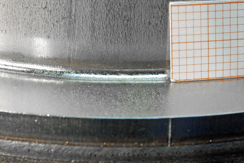
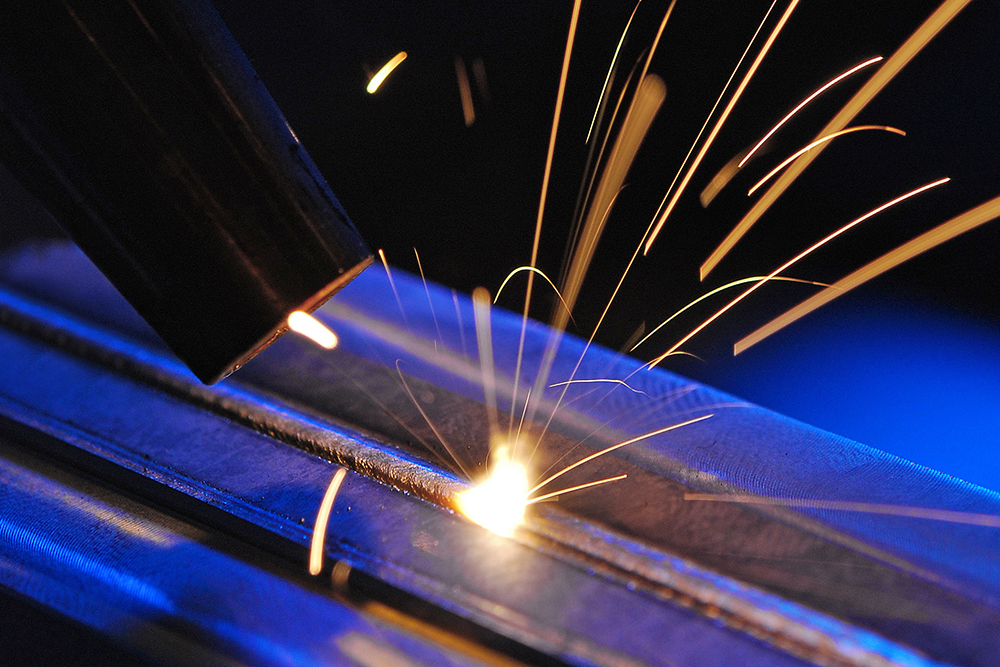
- Laser welding of reformers and microreactors,
- polymer welding used for applying a cover foil to polymer chips,
- ablation and cutting of polymers for lab-on-a-chip applications,
- ablation for the realization of microfluidic structures,
- metal stripping for the realization of conductor paths,
- micro drilling of polymers, metals and ceramics,
- 3D nanostructuring with 2-PA and interference lithography.